SEC Co., Ltd / SEC Europe Head Offcie / Nanotech Digital GmbH / Analysis report
semiconductor
Solder of PCB
For Automotive, EMS, Solder industrial
sne-4500m plus
Key Strength of Table-Top SEM(4500M Plus) system by SEC Co.,Ltd
Max. 150,000x of magnification by miniaturizing modules
Able to scan images with high resolution of 5nm
Various detectors which create surface information images (SE), and material information images (BSE)
Able to get images of variable angles via Tilting -45°~90°, and easily analyze EDS
User-friendly optimized U.I
High resolution
Fast vacuuming time
(3min)
Stage tilt
(-45 to 90 degree)
Easy to learn
Tabletop-SEM has been developed with compact design and minimization of Module for normal SEM. It is easy to use for everyone and has reasonable price. It is used for the purpose of development, quality assurance or etc in corporations, government offices and universities.
The image quality of the sample has decreased at the request of the client company.
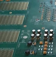
Generally, except in special cases, it is natural that solder points of PCB exist, and this causes many problems.
The sections of the solder pad and the solder ball that were taken with SEM are shown in the picture on the left below.
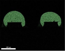
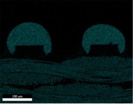
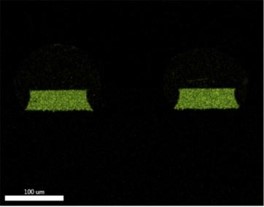
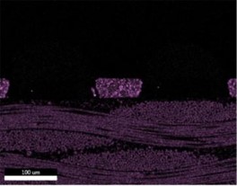
The boundary can be clearly checked by the difference in components, and it can be clearly identified through component analysis, as shown in the image on the right below.
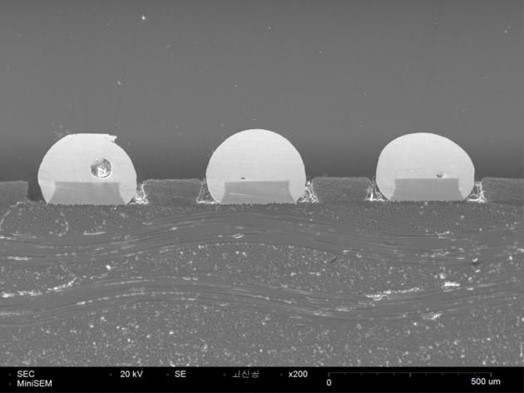
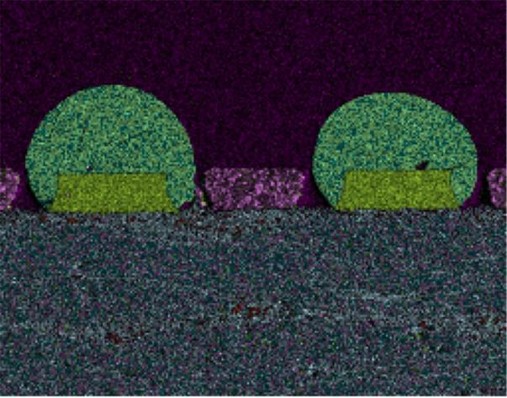
As shown in the images as bleow, the components of the Solder ball and pad can be identified through EDS (Energy Dispersive X-ray Spectrometer) analyses, and the images can be separately identified (the exact ingredients have been deleted by customer’s requirements).
