SEC Co., Ltd / SEC Europe Head Offcie / Nanotech Digital GmbH / Analysis report
semiconductor
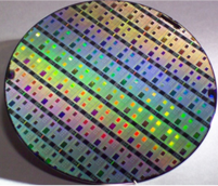
Nanopillars of WaferSE
For Solar cell, Battery, Nanoimprint
sne-4500m plus
Key Strength of Table-Top SEM(4500M Plus) system by SEC Co.,Ltd
Max. 150,000x of magnification by miniaturizing modules
Able to scan images with high resolution of 5nm
Various detectors which create surface information images (SE), and material information images (BSE)
Able to get images of variable angles via Tilting -45°~90°, and easily analyze EDS
User-friendly optimized U.I
High resolution
Fast vacuuming time
(3min)
Stage tilt
(-45 to 90 degree)
Easy to learn
Nanopillars have been sought after for many applications. For example, Si nanopillars have been used as nanoimprint lithography. also been used in solar cells and field-effect transistors.
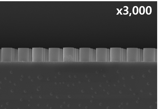
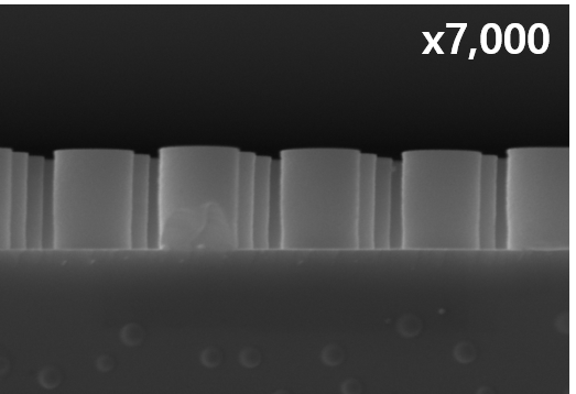
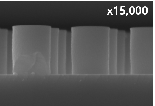
The shape of each nanopillar can be visualized in Table Top SEM of SEC as images below,
Showing a clear edge after the patterning and etching process.

It can know the surface, diameter, and height of the nanopillars, and it can also check the shape of the nanopillars.


It can be sufficiently used for research purposes or failure analysis by manufacturing new nanopillars. In addition, it is possible to obtain a satisfactory level of image compared to a high-performance SEM through a relatively inexpensive price.


